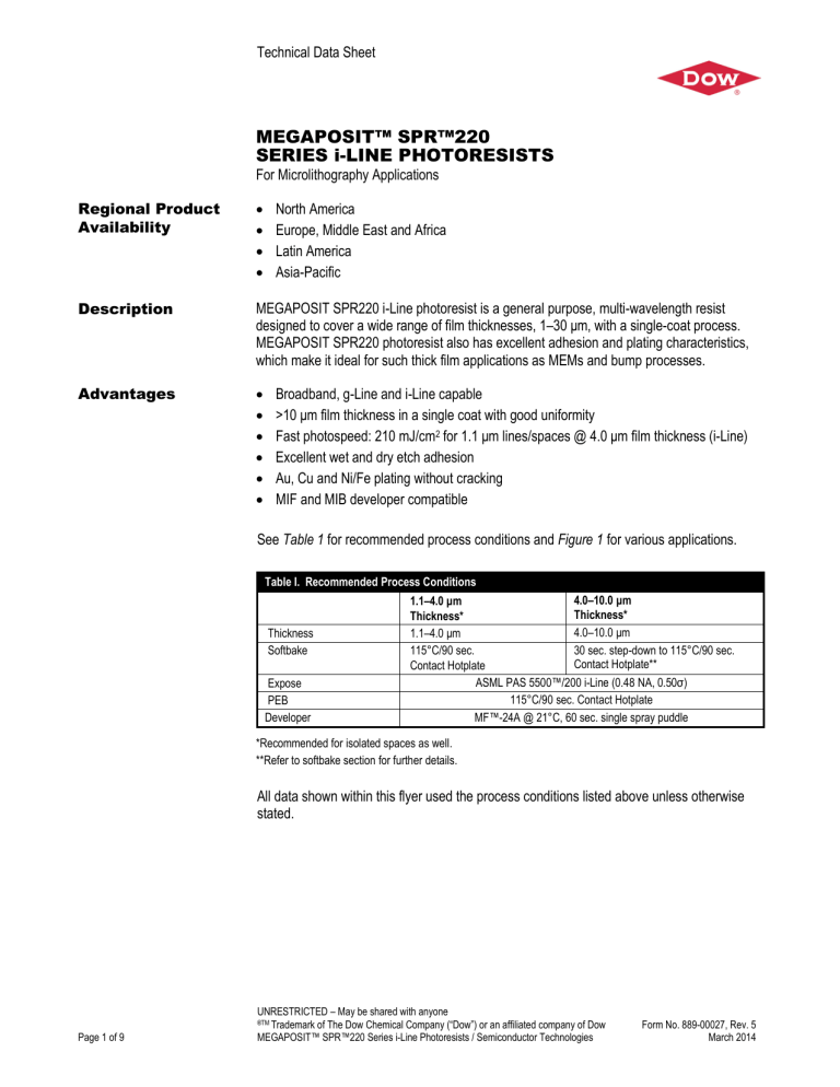
Technical Data Sheet MEGAPOSIT™ SPR™220 SERIES i-LINE PHOTORESISTS For Microlithography Applications Regional Product Availability • • • • Description MEGAPOSIT SPR220 i-Line photoresist is a general purpose, multi-wavelength resist designed to cover a wide range of film thicknesses, 1–30 μm, with a single-coat process. MEGAPOSIT SPR220 photoresist also has excellent adhesion and plating characteristics, which make it ideal for such thick film applications as MEMs and bump processes. Advantages • • • • • • North America Europe, Middle East and Africa Latin America Asia-Pacific Broadband, g-Line and i-Line capable >10 μm film thickness in a single coat with good uniformity Fast photospeed: 210 mJ/cm2 for 1.1 μm lines/spaces @ 4.0 μm film thickness (i-Line) Excellent wet and dry etch adhesion Au, Cu and Ni/Fe plating without cracking MIF and MIB developer compatible See Table 1 for recommended process conditions and Figure 1 for various applications. Table I. Recommended Process Conditions Thickness Softbake Expose PEB Developer 4.0–10.0 μm 1.1–4.0 μm Thickness* Thickness* 4.0–10.0 μm 1.1–4.0 μm 30 sec. step-down to 115°C/90 sec. 115°C/90 sec. Contact Hotplate** Contact Hotplate ASML PAS 5500™/200 i-Line (0.48 NA, 0.50σ) 115°C/90 sec. Contact Hotplate MF™-24A @ 21°C, 60 sec. single spray puddle *Recommended for isolated spaces as well. **Refer to softbake section for further details. All data shown within this flyer used the process conditions listed above unless otherwise stated. Page 1 of 9 UNRESTRICTED – May be shared with anyone of The Dow Chemical Company (“Dow”) or an affiliated company of Dow MEGAPOSIT™ SPR™220 Series i-Line Photoresists / Semiconductor Technologies ®TM Trademark Form No. 889-00027, Rev. 5 March 2014 Figure 1. Various Applications Table 2. Photospeed and Linearity of Dense Lines/Spaces at Various Thicknesses Film Thickness Photospeed* Linearity g-Line 1.2 μm 210 mJ/cm2 0.65 μm g-Line 3.0 μm 320 mJ/cm2 0.90 μm 7.0 μm 470 mJ/cm2 1.80 μm mJ/cm2 0.45 μm g-Line Page 2 of 9 i-Line 1.2 μm 160 i-Line 3.0 μm 310 mJ/cm2 0.90 μm i-Line 5.0 μm 380 mJ/cm2 0.90 μm UNRESTRICTED – May be shared with anyone of The Dow Chemical Company (“Dow”) or an affiliated company of Dow MEGAPOSIT™ SPR™220 Series i-Line Photoresists / Semiconductor Technologies ®TM Trademark Form No. 889-00027, Rev. 5 March 2014 Figure 2. Resolution at 3.0 μm Film Thickness Substrate MEGAPOSIT SPR220 photoresist is compatible with a wide range of substrates, including but not limited to silicon, aluminum oxide, gold, copper and nickel-iron. A hexamethyldisilizane (HMDS)-based MICROPOSIT™ primer is recommended to promote adhesion with substrates that require such treatment. Vacuum vapor priming at 120°C for 30 seconds with concentrated HMDS is recommended. Coat Figure 3 shows the relation between spin speed and resist thickness for 4-inch substrates. Figure 4 shows the relationship between spin speed and resist thickness for 8-inch (200 mm) substrates applying MEGAPOSIT SPR220-7.0 photoresist. Based on this curve a 375 RPM spin will yield a film thickness of approximately 30 μm. Nominal film thickness may vary slightly due to process, equipment and ambient conditions. Page 3 of 9 UNRESTRICTED – May be shared with anyone of The Dow Chemical Company (“Dow”) or an affiliated company of Dow MEGAPOSIT™ SPR™220 Series i-Line Photoresists / Semiconductor Technologies ®TM Trademark Form No. 889-00027, Rev. 5 March 2014 Figure 3. Spin Speed Curves on 4 in. Coat Uniformity @ 7.31 μm, standard deviation = 0.036 μm, (33 points) Figure 4. Spin Speed Curve, MEGAPOSIT SPR220-7.0 photoresist on 8 in. Softbake Page 4 of 9 The recommended softbake process for MEGAPOSIT SPR220 photoresist for films up to 4.0 μm is 115°C for 90 seconds on a contact hotplate. For films greater than 4.0 μm, use a 30 second ramp in temperature (stepdown to hotplate) to 115°C and hold for a minimum of 90 seconds. For film thickness greater than 12 μm, apply a 30 second ramp in temperature (step-down to hotplate) to 115°C and hold for a minimum of 300 sec. UNRESTRICTED – May be shared with anyone of The Dow Chemical Company (“Dow”) or an affiliated company of Dow MEGAPOSIT™ SPR™220 Series i-Line Photoresists / Semiconductor Technologies ®TM Trademark Form No. 889-00027, Rev. 5 March 2014 Film Thickness Measurement Figure 5 shows the refractive index of MEGAPOSIT SPR220 photoresist as a function of wavelength. Cauchy coefficients are listed in Table 3. Refractive index and dill parameters are listed in Table 4 and Table 5, respectively. For film thickness greater than 12 μm the resist is exposed to an energy dose between 700 and 1,300 mJ/cm2 (measured using standard radiometer @ 365 nm wavelength) using a high energy light source that generates peak output of wavelengths between 350 to 400 nm. Coating uniformity and the applied soft bake parameters can affect the required exposure energy needed for standardization and determination of the optimized exposure. Figure 5. Dispersion Curve Table 3. Cauchy Coefficients n1 1.6035 n2 9.7122e+5 n3 8.2082e+12 Table 4. Refractive Index RI @ 365 nm 1.73 RI @ 405 nm 1.70 RI @ 436 nm 1.67 RI @ 633 nm 1.63 Table 5. Dill Parameters Page 5 of 9 365 nm 405 nm 436 nm Dill A 0.5250 0.7075 0.4242 Dill B 0.0298 0.0173 0.0150 UNRESTRICTED – May be shared with anyone of The Dow Chemical Company (“Dow”) or an affiliated company of Dow MEGAPOSIT™ SPR™220 Series i-Line Photoresists / Semiconductor Technologies ®TM Trademark Form No. 889-00027, Rev. 5 March 2014 Expose The absorbance curves for the unexposed and exposed resist film are shown in Figure 6. Post-Exposure Bake Post-exposure bake (PEB) is run at the same temperature as the softbake. With thicker films (above 4 μm), a hold time is used between exposure and PEB to allow water (which is necessary to complete the photo-reaction) to diffuse back into the photoresist film. Thick films should use a minimum hold time of 35 minutes. A film thickness greater than 12 μm requires a minimum hold time of 120 minutes between exposure and develop should be applied. Figure 6. Absorbance Curves Develop MEGAPOSIT SPR220 photoresist is optimized for 0.24N developers. Thicker films or highthroughput processes can utilize 0.26N developers. MEGAPOSIT SPR220 photoresist has also been formulated for use in metal-ion free and metal-ion bearing developers, as demonstrated in Figure 7. See Table 6 for recommended develop conditions. Table 6. Recommended Develop Conditions Page 6 of 9 1.2 μm FT 3.0 μm FT 5.0 μm FT 7.0 μm FT MF-24A 40 sec. SP 60 sec. SP 60/60 sec. DP 60/60 sec. DP MF-26A 40 sec. SP 60 sec. SP 80 sec. SP 60/60 sec. DP M452 — 3 min. Imm 3 min. Imm. 3 min. Imm. M453 — — 3 min. Imm. 3 min. Imm. UNRESTRICTED – May be shared with anyone of The Dow Chemical Company (“Dow”) or an affiliated company of Dow MEGAPOSIT™ SPR™220 Series i-Line Photoresists / Semiconductor Technologies ®TM Trademark Form No. 889-00027, Rev. 5 March 2014 Figure 7. Developer Compatibility For thick film application 12 μm or greater using MF-26A developer, the overall development time will behave similar to the thin film time cited in Figure 7 above. Etch Resistance Figure 8 shows the etch performance of SPR220 with a Bosch Etch process (100:1 etch selectivity). Figure 8. Etch Performance Page 7 of 9 UNRESTRICTED – May be shared with anyone of The Dow Chemical Company (“Dow”) or an affiliated company of Dow MEGAPOSIT™ SPR™220 Series i-Line Photoresists / Semiconductor Technologies ®TM Trademark Form No. 889-00027, Rev. 5 March 2014 Photoresist Removal Page 8 of 9 MEGAPOSIT SPR220 photoresist can be removed with MICROPOSIT REMOVER 1165. A two-bath process is recommended with each bath at a temperature of 80°C (176°F). The first bath removes the bulk of the photoresist and the second removes residual traces of photoresist. Please consult specific remover data sheets for additional process information. UNRESTRICTED – May be shared with anyone of The Dow Chemical Company (“Dow”) or an affiliated company of Dow MEGAPOSIT™ SPR™220 Series i-Line Photoresists / Semiconductor Technologies ®TM Trademark Form No. 889-00027, Rev. 5 March 2014 Handling Precautions Before using this product, associated generic chemicals or the analytical reagents required for its control, consult the supplier's Material Safety Data Sheet (MSDS)/Safety Data Sheet (SDS) for details on material hazards, recommended handling precautions and product storage. CAUTION! Keep combustible and/or flammable products and their vapors away from heat, sparks, flames and other sources of ignition including static discharge. Processing or operating at temperatures near or above product flashpoint may pose a fire hazard. Use appropriate grounding and bonding techniques to manage static discharge hazards. CAUTION! Failure to maintain proper volume level when using immersion heaters can expose tank and solution to excessive heat resulting in a possible combustion hazard, particularly when plastic tanks are used. Storage Store products in tightly closed original containers at temperatures recommended on the product label. Disposal Considerations Dispose in accordance with all local, state (provincial) and federal regulations. Empty containers may contain hazardous residues. This material and its container must be disposed in a safe and legal manner. It is the user's responsibility to verify that treatment and disposal procedures comply with local, state (provincial) and federal regulations. Contact your Dow Electronic Materials Technical Representative for more information. Product Stewardship Dow has a fundamental concern for all who make, distribute, and use its products, and for the environment in which we live. This concern is the basis for our product stewardship philosophy by which we assess the safety, health, and environmental information on our products and then take appropriate steps to protect employee and public health and our environment. The success of our product stewardship program rests with each and every individual involved with Dow products - from the initial concept and research, to manufacture, use, sale, disposal, and recycle of each product. Customer Notice Dow strongly encourages its customers to review both their manufacturing processes and their applications of Dow products from the standpoint of human health and environmental quality to ensure that Dow products are not used in ways for which they are not intended or tested. Dow personnel are available to answer your questions and to provide reasonable technical support. Dow product literature, including safety data sheets, should be consulted prior to use of Dow products. Current safety data sheets are available from Dow. For Industrial Use Only. This information is based on our experience and is, to the best of our knowledge, true and accurate. However, since conditions for use and handling of products are beyond our control, we make no guarantee or warranty, expressed or implied, regarding the information, the use, handling, storage or possession of the products, or the applications of any process described herein or the results sought to be obtained. Nothing herein shall be construed as a recommendation to use any product in violation of any patent rights. Contact: North America: 1-800-832-6200 Taiwan: 886-37-539100 China: (+86) 21-3851-1000 Hong Kong: (+852) 2879-7333 Korea: (+82) 2-3490-0700 Japan: (+81) 3-5460-2200 Europe: (+41)(0)44-728-2111 www.dowelectronicmaterials.com Page 9 of 9 NOTICE: No freedom from infringement of any patent owned by Dow or others is to be inferred. Because use conditions and applicable laws may differ from one location to another and may change with time, Customer is responsible for determining whether products and the information in this document are appropriate for Customer's use and for ensuring that Customer's workplace and disposal practices are in compliance with applicable laws and other government enactments. The product shown in this literature may not be available for sale and/or available in all geographies where Dow is represented. The claims made may not have been approved for use in all countries. Dow assumes no obligation or liability for the information in this document. References to “Dow” or the “Company” mean the Dow legal entity selling the products to Customer unless otherwise expressly noted. NO WARRANTIES ARE GIVEN; ALL IMPLIED WARRANTIES OF MERCHANTABILITY OR FITNESS FOR A PARTICULAR PURPOSE ARE EXPRESSLY EXCLUDED. UNRESTRICTED – May be shared with anyone ®TM Trademark of The Dow Chemical Company (“Dow”) or an affiliated company of Dow MEGAPOSIT™ SPR™220 Series i-Line Photoresists / Semiconductor Technologies Form No. 889-00027, Rev. 5 March 2014
