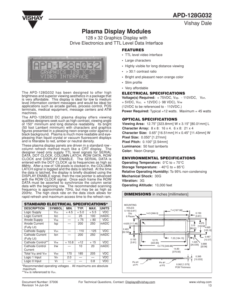
APD-128G032 Vishay Dale Plasma Display Modules 128 x 32 Graphics Display with Drive Electronics and TTL Level Data Interface FEATURES • TTL level video interface • Large characters • Highly visible for long distance viewing • > 30:1 contrast ratio • Bright and pleasant neon orange color • Slim profile • Very affordable The APD-128G032 has been designed to offer high brightness and superior viewing aesthetics in a package that is very affordable. This display is ideal for low to medium level information content messages and would be ideal for applications such as arcade games, process control, POS terminals, medical equipment, message centers and ATM machines. The APD-128G032 DC plasma display offers viewing qualities designers seek such as high contrast, viewing angle of 150° minimum and long distance readability. Its bright (50 foot Lambert minimum) with characters and graphics figures presented in a pleasing neon orange color against a black background. Plasma is much more readable and eyepleasing than liquid crystal or vacuum fluorescent displays and is filterable to red, amber or neutral density. These plasma display panels are driven in a standard row column refresh method much like a CRT display. The designer need only supply TTL level signals for SERIAL DATA, DOT CLOCK, COLUMN LATCH, ROW DATA, ROW CLOCK and DISPLAY ENABLE. The SERIAL DATA is entered with the DOT CLOCK up to frequencies as high as 8MHz. After a row of 128 pixels is clocked in, the COLUMN LATCH signal is toggled and the data is latched. At the time the data is latched, the display is briefly disabled using the DISPLAY ENABLE signal, then the row pointer is advanced with the ROW CLOCK signal. Once each frame the ROW DATA must be asserted to synchronize the column serial data with the beginning row. The recommended scanning frequency is approximately 70Hz, but may be as high as 200Hz. The high clock rate on the data clock allows for rapid refresh and maximum access time to the refresh ram. STANDARD ELECTRICAL SPECIFICATIONS* DESCRIPTION SYMBOL MIN. Logic Supply Vcc + 4.5 Logic Current Icc — Anode Supply Vsp — Anode Current Isp — (Fully Lit) Cathode Supply Vsn — Cathode Current Isn — (Fully Lit) Cathode Control** Vrw + 10.8 Cathode Control Irw — Current Total Vsp and Vsn Vtot 170 Logic 1 Input Vih 2.0 Logic 0 Input Vil — TYP. + 5.0 25 + 75 200 MAX. + 5.5 100 + 80 250 UNITS VDC mADC VDC mADC - 110 200 - 125 250 VDC mADC +12 10 + 15 20 VDC mADC 185 — — 205 — 0.8 VDC VDC VDC *Recommended operating voltages . All maximums are absolute maximum. **Vrw is referenced to Vsn. Document Number: 37006 Revision 14-Jun-04 ELECTRICAL SPECIFICATIONS Voltage(s) Required: + 75VDC, Vsp. - 110VDC, Vsn. + 5VDC, Vcc. + 12VDC (- 98 VDC), Vrw (12VDC to be referenced to - 110VDC.) Power Required: Typical =12 watts. Maximum = 45 watts OPTICAL SPECIFICATIONS Viewing Area: 12.75" [323.8mm] W x 3.15" [80.01mm] L Character Array: 8 x 8: 16 x 4. 6 x 8: 21 x 4 Character Size: 0.65" [16.51mm] H x 0.45" [11.43mm] W Pixel Size: 0.050" [1.27mm] Pixel Pitch: 0.100" [2.54mm] Luminance: 50 foot lamberts Color: Neon Orange ENVIRONMENTAL SPECIFICATIONS Operating Temperature: 0°C to + 70°C Storage Temperature: - 40°C to + 85°C Relative Operating Humidity: To 95% non-condensing Mechanical Shock: 30G Vibration: 3G Operating Altitude: 10,000 feet DIMENSIONS in inches [millimeters] MOUNTING HOLES 0.150 [3.81] Dia. 6 Places 7.4 [187.96] 0.150 [3.81] 14.5 [368.3] 4.075 3.15 [103.50] 4.925 [80.01] [125.10] 4.625 [117.48] 2.463 [62.56] 0.150 [3.81] 0.487 [12.37] 7.25 [184.15] 12.75 [323.85] 13.775 [349.88] 14.80 [375.92] 1.025 [26.035] 0.888 [22.56] 0.395 [10.033] Pin #1 of P1 For Technical Questions, Contact: Displays@vishay.com Pin #1 of P2 0.062 [1.575] PCB Thickness www.vishay.com 13 APD-128G032 Vishay Dale PIN DESCRIPTION LOGIC AND DATA TIMING P1 - POWER CONNECTOR AMP #640445-8 or equivalent. Mates with AMP 640428-8, MOLEX 09-50-3081 or equivalent. PIN SIGNAL DESCRIPTION 1 Vsn Cathode supply 2 Vrw Cathode control 3 KEY Used to key connector 4 GND Vsn and Vsp 5 GND Vcc 6 Vcc Logic supply 7 NOT USED 8 Vsp Anode supply P2 - DATA CONNECTOR AMP #103309-2 or equivalent. Mates with AMP 746195-2, MOLEX 39-27-1146 or equivalent. PIN DESCRIPTION PIN DESCRIPTION 1 DISPLAY ENABLE 2 GROUND 3 ROW DATA 4 GROUND 5 ROW CLOCK 6 GROUND 7 COLUMN LATCH 8 GROUND 9 DOT CLOCK 10 GROUND 11 SERIAL DATA 12 GROUND 13 No connect 14 GROUND t4 Row Data t2 t3 t1 Row Clock 0 0 2 1 1 30 2 31 30 31 0 0 1 1 Display Enable Row Clock Column Latch INTERFACE SIGNAL DESCRIPTION DOT CLOCK - This signal enters the SERIAL DATA on each low to high transition. A total of 128 DOT CLOCK transitions must be present for each line of column/anode data. SERIAL DATA - This signal presents the pixel data in positive logic format. A logic one represents a lit pixel and a logic zero represents an extinguished pixel. Data is entered from right to left. The first pixel data entered will represent the left most pixel in the row. COLUMN LATCH - This signal latches the pixel data into the driver outputs. When the COLUMN LATCH signal goes to logic one the data entered previously will fall through to the driver outputs. When the signal returns to a logic zero the data is latched and the shift register is now ready to accept the next row of data. Must be held low while entering new SERIAL DATA. DISPLAY ENABLE - This signal enables the output drivers. Using a duty cycle control, this signal may also be used for intensity control. The DISPLAY ENABLE must be at logic zero before the COLUMN LATCH signal transitions. To avoid display blurring, the ROW CLOCK signal should also transition while DISPLAY ENABLE is a logic zero. ROW DATA - This signal is the first line marker for the scan. This input should be held high to correspond to the first row of pixel data. ROW CLOCK - This signal clocks ROW DATA on the falling edge. The ROW CLOCK signal is repetitive and must be present for proper scanning of the display module. The APD-128G032 has an unique input protection circuit that assures the column drivers stay blanked on power up. The protection circuit unblanks the column drivers when the ROW CLOCK signal begins (i.e the display begins scanning.) www.vishay.com 14 Display Enable 1st bit of row will appear in leftmost column Serial Data 1 0 2 126 127 t5 Dot Clock t6 PARAMETER t1 t2 Positive Edge x 128 t7 MINIMUM 100 TYPICAL - MAXIMUM - UNITS nS uS 5 - - t3 1 - - uS t4 - 70 200 Hz t5 25 - - nS t6 75 - - nS t7 75 - - nS ORDERING INFORMATION DESCRIPTION PART NUMBER Display, Driver Electronics and TTL Interface ..... APD-128G032 Data Connector Kit .................................................... 280105-05 Power Connector Kit .................................................. 280108-12 DC/DC Converter Assembly ...................................... 280961-03 For Technical Questions, Contact: Displays@vishay.com Document Number: 37006 Revision 14-Jun-04 Legal Disclaimer Notice Vishay Disclaimer All product specifications and data are subject to change without notice. Vishay Intertechnology, Inc., its affiliates, agents, and employees, and all persons acting on its or their behalf (collectively, “Vishay”), disclaim any and all liability for any errors, inaccuracies or incompleteness contained herein or in any other disclosure relating to any product. Vishay disclaims any and all liability arising out of the use or application of any product described herein or of any information provided herein to the maximum extent permitted by law. The product specifications do not expand or otherwise modify Vishay’s terms and conditions of purchase, including but not limited to the warranty expressed therein, which apply to these products. No license, express or implied, by estoppel or otherwise, to any intellectual property rights is granted by this document or by any conduct of Vishay. The products shown herein are not designed for use in medical, life-saving, or life-sustaining applications unless otherwise expressly indicated. Customers using or selling Vishay products not expressly indicated for use in such applications do so entirely at their own risk and agree to fully indemnify Vishay for any damages arising or resulting from such use or sale. Please contact authorized Vishay personnel to obtain written terms and conditions regarding products designed for such applications. Product names and markings noted herein may be trademarks of their respective owners. Document Number: 91000 Revision: 18-Jul-08 www.vishay.com 1
