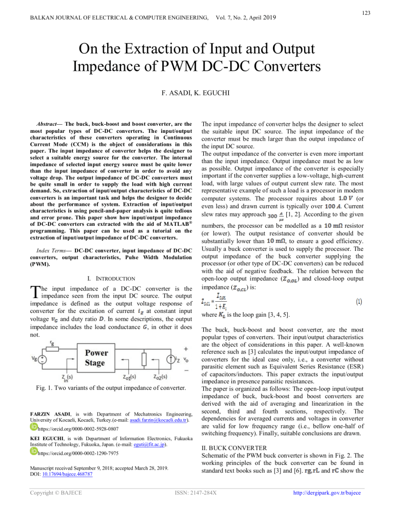
BALKAN JOURNAL OF ELECTRICAL & COMPUTER ENGINEERING, 123 Vol. 7, No. 2, April 2019 On the Extraction of Input and Output Impedance of PWM DC-DC Converters F. ASADI, K. EGUCHI Abstract— The buck, buck-boost and boost converter, are the most popular types of DC-DC converters. The input/output characteristics of these converters operating in Continuous Current Mode (CCM) is the object of considerations in this paper. The input impedance of converter helps the designer to select a suitable energy source for the converter. The internal impedance of selected input energy source must be quite lower than the input impedance of converter in order to avoid any voltage drop. The output impedance of DC-DC converters must be quite small in order to supply the load with high current demand. So, extraction of input/output characteristics of DC-DC converters is an important task and helps the designer to decide about the performance of system. Extraction of input/output characteristics is using pencil-and-paper analysis is quite tedious and error prone. This paper show how input/output impedance of DC-DC converters can extracted with the aid of MATLAB ® programming. This paper can be used as a tutorial on the extraction of input/output impedance of DC-DC converters. Index Terms— DC-DC converter, input impedance of DC-DC converters, output characteristics, Pulse Width Modulation (PWM). I. INTRODUCTION T he input impedance of a DC-DC converter is the impedance seen from the input DC source. The output impedance is defined as the output voltage response of converter for the excitation of current at constant input voltage and duty ratio . In some descriptions, the output impedance includes the load conductance , in other it does not. Fig. 1. Two variants of the output impedance of converter. FARZIN ASADI, is with Department of Mechatronics Engineering, University of Kocaeli, Kocaeli, Turkey.(e-mail: asadi.farzin@kocaeli.edu.tr). https://orcid.org/0000-0002-5928-0807 KEI EGUCHI, is with Department of Information Electronics, Fukuoka Institute of Technology, Fukuoka, Japan. (e-mail: eguti@fit.ac.jp). https://orcid.org/0000-0002-1290-7975 Manuscript received September 9, 2018; accepted March 28, 2019. DOI: 10.17694/bajece.468787 Copyright © BAJECE The input impedance of converter helps the designer to select the suitable input DC source. The input impedance of the converter must be much larger than the output impedance of the input DC source. The output impedance of the converter is even more important than the input impedance. Output impedance must be as low as possible. Output impedance of the converter is especially important if the converter supplies a low-voltage, high-current load, with large values of output current slew rate. The most representative example of such a load is a processor in modern computer systems. The processor requires about (or even less) and drawn current is typically over . Current slew rates may approach [1, 2]. According to the given numbers, the processor can be modelled as a resistor (or lower). The output resistance of converter should be substantially lower than , to ensure a good efficiency. Usually a buck converter is used to supply the processor. The output impedance of the buck converter supplying the processor (or other type of DC-DC converters) can be reduced with the aid of negative feedback. The relation between the open-loop output impedance ( ) and closed-loop output impedance ( ) is: where is the loop gain [3, 4, 5]. The buck, buck-boost and boost converter, are the most popular types of converters. Their input/output characteristics are the object of considerations in this paper. A well-known reference such as [3] calculates the input/output impedance of converters for the ideal case only, i.e., a converter without parasitic element such as Equivalent Series Resistance (ESR) of capacitors/inductors. This paper extracts the input/output impedance in presence parasitic resistances. The paper is organized as follows: The open-loop input/output impedance of buck, buck-boost and boost converters are derived with the aid of averaging and linearization in the second, third and fourth sections, respectively. The dependencies for averaged currents and voltages in converter are valid for low frequency range (i.e., bellow one-half of switching frequency). Finally, suitable conclusions are drawn. II. BUCK CONVERTER Schematic of the PWM buck converter is shown in Fig. 2. The working principles of the buck converter can be found in standard text books such as [3] and [6]. and show the ISSN: 2147-284X http://dergipark.gov.tr/bajece BALKAN JOURNAL OF ELECTRICAL & COMPUTER ENGINEERING, internal resistance of the input DC source, inductor ESR and capacitor ESR, respectively. 124 Vol. 7, No. 2, April 2019 According to Fig. 4, the circuit differential equations can be written as: Fig. 2. Schematic of PWM buck converter. When the MOSFET switch is closed, the diode is reversebiased and the equivalent circuit of Fig. 3 applies. shows the MOSFET drain-source resistance. is a fictitious current source added to the circuit in order to measure the output impedance ( ). Fig. 3. Equivalent circuit of buck converter with closed MOSFET. According to Fig. 3, the circuit differential equations can be written as: State Space Averaging (SSA) is one of the most important tools to study the dynamics of converters operating in CCM. Foundation of SSA was laid down in [7] and later extended in [8, 9, 10], as well as many other publications. Theory of SSA has been studied in many text books for instance see [10] and [11]. SSA has two important steps: averaging and linearization. The SSA procedure can be summarized as follows [11]: Step 1- Circuit differential equations are written for different working modes (i.e on/off state of semiconductor switches). Step 2- Equations are time averaged over one period. Step 3- Steady state operating points are calculated by equating the derivative terms to zero. Step 4- The averaged equations are linearized around the steady state operating point found in the third step. Applying the SSA to the Equations (2)-(9) leads to 6 different transfer functions: and . Openloop input and output impedance of the converter is extracted with the aid of and , respectively. Applying the aforementioned steps manually is tedious and error prone (especially if the converter order is high). MATLAB® can be very helpful to do the mathematical machinery of SSA. The program shown in appendix (program 1) extracts the small signal transfer functions of a buck converter with component values as shown in Table 1. When the MOSFET is open, the diode becomes forwardbiased to carry the inductor current and the equivalent circuit of Fig. 4 applies. and show the diode resistance and diode forward voltage drop, respectively. Fig. 4. Equivalent circuit of buck converter with open MOSFET. Copyright © BAJECE Table I . The buck converter parameters (see Fig. 2). Nominal Value Output voltage, vo 20 V Duty ratio, D 0.4 Input DC source voltage, Vg 50 V Input DC source internal resistance, rg 0.01 Ω MOSFET Drain-Source resistance, rds 40 mΩ Capacitor, C 100 μF Capacitor ESR, rC 0.05 Ω Inductor, L 400 μH Inductor ESR, rL 50 mΩ Diode voltage drop, vD 0.7 V Diode forward resistance, rD 10 mΩ Load resistor, R 20 Ω Switching Frequency, Fsw 20 kHz ISSN: 2147-284X http://dergipark.gov.tr/bajece 125 Vol. 7, No. 2, April 2019 BALKAN JOURNAL OF ELECTRICAL & COMPUTER ENGINEERING, The program gives the following results (OL sub script stands for Open Loop): Bode diagram of control-to-output transfer function, open loop input impedance and open loop output impedance are shown in Fig. 5, 6 and 7, respectively. Fig. 8. Dynamical model of the studied buck converter. Input voltage variations are ignored. Consider a simple feedback loop as shown in Fig. 9. Fig. 5. Control-to-output transfer function of studied buck converter. Fig. 9. Voltage Mode (VM) control of the studied buck converter. Assume that the controller is a simple I-type controller ( ). Fig. 10, shows the step response of the closed loop. Fig. 6. Open loop input impedance of studied buck converter. Fig. 7. Open loop output impedance of studied buck converter. The block diagram shown in Fig. 8 can be drawn for the studied buck converter. We want to study the effect of feedback on output impedance. Fig. 10. Step response of closed-loop control system shown in Fig. 9 with . Copyright © BAJECE ISSN: 2147-284X http://dergipark.gov.tr/bajece BALKAN JOURNAL OF ELECTRICAL & COMPUTER ENGINEERING, 126 Vol. 7, No. 2, April 2019 According to Fig. 9, the closed loop output impedance ( ) is: Fig. 12. Schematic of PWM buck-boost converter. When the MOSFET is closed, the diode is reverse biased. Fig. 11, is a comparison between the open-loop output impedance ( , Equation (12)) and closed-loop output impedance ( , Equation (14)). The closed loop output impedance is reduced at low frequency portion of the graph. Reduction of output impedance is one of the desired properties of feedback control. Fig. 13. Equivalent circuit of buck-boost converter with closed MOSFET. According to Fig. 13, the circuit differential equations can be written as: Fig. 11. Comparison of open-loop output impedance with closed-loop output impedance for the studied buck converter. There are many efforts presented in the literature to achieve satisfactory output impedance of PWM DC-DC converters, especially buck type. The methods can be categorized into two groups: Sophisticated design of control loops in the converter [13, 14, 15, 16] Modifications of the basic structure of the power stage [17-18]. The starting point of the first method is the precise description of the converter, in particular the use of accurate formulas for open-loop output impedance. The program given in appendix can be helpful for this purpose [19]. III. BUCK-BOOST CONVERTER Schematic of the buck-boost converter is shown in Fig. 12. Copyright © BAJECE When the MOSFET switch is opened, the diode becomes forward-biased. Fig. 14. Equivalent circuit of buck-boost converter with open MOSFET. According to Fig. 14, the circuit differential equations can be written as: ISSN: 2147-284X http://dergipark.gov.tr/bajece BALKAN JOURNAL OF ELECTRICAL & COMPUTER ENGINEERING, 127 Vol. 7, No. 2, April 2019 The program shown in appendix (program 2) extracts the small signal transfer functions of a buck-boost converter with component values as shown in Table 2. Table II. The buck-boost converter parameters (see Fig. 12). Nominal Value Output voltage, vo -16 V Duty ratio, D 0.4 Input DC source voltage, Vg 24 V Input DC source internal resistance, rg 0.1 Ω MOSFET Drain-Source resistance, rds 40 mΩ Capacitor, C 80 μF Capacitor ESR, rC 0.05 Ω Inductor, L 20 μH Inductor ESR, rL 10 mΩ Diode voltage drop, vD 0.7 V Diode forward resistance, rD 10 mΩ Load resistor, R 5Ω Switching Frequency, Fsw 100 kHz Fig. 16. Open loop input impedance of studied buck-boost converter. The program gives the following results: Fig. 17. Open loop output impedance of studied buck-boost converter. Bode diagram of control-to-output transfer function, open loop input impedance and open loop output impedance are shown in Fig. 15, 16 and 17, respectively. IV. BOOST CONVERTER Schematic of boost converter is shown in Fig. 18. Fig. 18. Schematic of PWM boost converter. When the MOSFET is closed, the diode is reverse biased. Fig. 15. Control-to-output transfer function of studied buckboost converter. Copyright © BAJECE ISSN: 2147-284X http://dergipark.gov.tr/bajece BALKAN JOURNAL OF ELECTRICAL & COMPUTER ENGINEERING, 128 Vol. 7, No. 2, April 2019 Table III. The boost converter parameters (see Fig. 18). Nominal Value Fig. 19. Equivalent circuit of boost converter with closed MOSFET. According to Fig. 19, the circuit differential equations can be written as: Output voltage, vo 30 V Duty ratio, D Input DC source voltage, Vg 0.6 12 V Input DC source internal resistance, rg MOSFET Drain-Source resistance, rds Capacitor, C Capacitor ESR, rC Inductor, L Inductor ESR, rL Diode voltage drop, vD Diode forward resistance, rD Load resistor, R The program gives the following results: 0.1 Ω 40 mΩ 100 μF 0.05 Ω 120 μH 10 mΩ 0.7 V 10 mΩ 50 Ω When the MOSFET switch is opened, the diode becomes forward-biased. Fig. 20, shows the equivalent circuit for this case. Bode diagram of control-to-output transfer function, open loop input impedance and open loop output impedance are shown in Fig. 21, 22 and 23, respectively. Fig. 20. Equivalent circuit of boost converter with open MOSFET. According to Fig. 20, the circuit differential equations can be written as: Fig. 21. Control-to-output transfer function of studied boost converter The program shown in appendix (program 3) extracts the small signal transfer functions of a boost converter with component values as shown in Table 3. Switching Frequencyis 25 kHz. Copyright © BAJECE ISSN: 2147-284X http://dergipark.gov.tr/bajece BALKAN JOURNAL OF ELECTRICAL & COMPUTER ENGINEERING, 129 Vol. 7, No. 2, April 2019 This paper studied the input/output characteristics of buck, buck-boost and boost converters. MATLAB programming is used to do the mathematical machinery. Input/output characteristics of other types of converters can be extracted in a similar way shown in the paper. The control to output transfer function of power electronics converters is used to design the control loop of converter. The Buck converter has a minimum phase control to output transfer function while the Boost and Buck-Boost converters have non-minimum phase control to output transfer functions. The feedback control of power converters affect the output impedance of converter. The output impedance of converter decreases with the aid of feedback control as shown in the second sectiom of paper. REFERENCES Fig. 22. Open loop input impedance of studied boost converter. [1] Voltage Regulator Module (VRM) and Enterprise Voltage Regulator-Down (EVRD), 11.1 Design Guidelines, Intel Corp.,2009. [2] R.P. Singh and A.M. Khambadkone, “A Buck-derived topology with improved step-down transient response”, IEEE Trans. on Power Electronics 23 (6), 2855–2866 (2008). [3] R.W. Erickson and D. Maksimovic, Fundamentals of Power Electronics, 2-nd Ed., Kluwer, Berlin, 2002. [4] K. Yao, M. Xu, Y. Meng, and F.C. Lee, “Design considerations for VRM transient response based on the output imedance”, IEEE Trans. on Power Electronics 18 (6), 1270–1277 (2003). Fig. 23. Open loop output impedance of studied boost converter. The programs given in appendix calculates the steady state operating point of the converters as well. The steady state operating point for studied boost converter is and . and show the average inductor current and average capacitor voltage, respectively. The average current drawn from the input DC source is the same as the average current of inductor. So, the input DC source sees the converter as a load. If we substitute in the Equation (35), we obtain the which is quite close to the expected value. The DC gain of obtained input impedance (at ) can be checked in a similar way for other type of converters. V. CONCLUSION Input/output characteristics of DC-DC converters are important parameters. The input impedance helps the designer to select the suitable input source. The output impedance of the converter shows whether the converter can supply the output load successfully or not. Copyright © BAJECE [5] R. Ahmadi, D. Paschedag, and M. Ferdowsi, “Closed loop input and output impedances of DC-DC switching converters operating in voltage and current mode control”, IECON 36-th Annual Conf. IEEE Industrial Electronic Society 1, 2311– 2316 (2010). [6] M.K. Kazimierczuk, Pulse-Width Modulated DC – DC Power Converters, J. Wiley, London, 2008. [7] Middlebrook RD, Cuk S. A general unified approach to modeling switching-converter power stages. Int. J. Electronics Theoretical and Experimental.1977.p. 521–550. [8] Tymerski R, Vorperian V. Generation, classification and analysis of switched-mode DC-DC converters by the use of converter cells. Telecommunications Energy Conference. 1986. p. 181-195. [9] Chen J, Ngo K.D.T. Alternate forms of the PWM switch model in discontinuous conduction mode. IEEE Trans. Aerosp. Electron. Syst. 2001.p. 754-758. [10] Sun J, Mitchell DM, Greuel MF, Krein PT, Bass RM. Average modeling of PWM converters in discontinuous modes. IEEE Trans. Power Electron. 2001.p. 482–492. ISSN: 2147-284X http://dergipark.gov.tr/bajece BALKAN JOURNAL OF ELECTRICAL & COMPUTER ENGINEERING, [11] Asadi F, Eguchi K. Dynamics and control of DC-DC converters, San Rafael: Morgan and Claypool; 2018. p. 89145. [12] Suntio T. Dynamic profile of switched mode converter: modeling, analysis and control. New Jersy: John Wiley & Sons. 2009. p. 17-37. [13] D. Chen, F.C. Lee, and S.J. Chen, “Evaluation of various Adaptive Voltage Positioning (AVP) schemes for computer power sources”, J. Chinese Institution of Engineers 30 (7), 1137–1143 (2007). [14] M. Lee, D.C. Huang, K. Chih-Wen, and L. Ben Tai, “Modeling and design for a novel adaptive voltage positioning (AVP) scheme for multiphase VRM”, IEEE Trans. on Power Electronics 23 (4), 1733–1742 (2008). 130 Vol. 7, No. 2, April 2019 ICICIC2017 Best Paper Award, ICICIC2016 Best Paper Award, ICEEI2016 Excellent Oral Presentation Award, ICIAE2016 Best Presentation Award, ICEESE2016 Best Presenter Award, ICIAE2015 Best Presentation Award, ICPEE2014 Excellent Oral Presentation Award, iCABSE2014 Excellent Paper Award, KKU-IENC2014 Outstanding Paper Award, ICEEN2014 Excellent Paper Award, JTL-AEME2013 Best Paper Award, ICTEEP2013 Best Session Paper Award, 2010 Takayanagi Research Encourage Award, 2010 Paper Award of Japan Society of Technology Education, ICICIC2009 Best Paper Award, and ICINIS2009 Outstanding Contribution Award. He is a senior member of IEEJ and a member of INASS, and JSTE. His research interests include nonlinear dynamical systems, intelligent circuits and systems, and low-voltage analog integrated circuits. [15] S. Xiao, W. Qiu, G. Miller, T.X. Wu, and I. Batarseh, “Adaptive modulation control for multiple-phase voltage regulators”, IEEE Trans. on Power Electronics 23 (1), 495– 499 (2008). [16] J.A. Qahouq and V.P. Arikatla, “Power converter with digital sensorless adaptive voltage positioning control scheme”, IEEE Trans. on Industrial Electronics 58 (9), 4105– 4116 (2011). [17] R.P. Singh and A.M. Khambadkone, “A Buck-derived topology with improved step-down transient response”, IEEE Trans.on Power Electronics 23 (6), 2855–2866 (2008). [18] Y. Birbir, and M. Yilmaz. "Optimal Speed Application on the Universal Motor by Means of Microcontroller." WSEAS Transactions on Power Systems 1.11 (2006): 1903. [19] M.E. Asker, and H. Kilic. "Modulation Index and Switching Frequency Effect on Symmetric Regular Sampled SPWM." European Journal of Technique 7.2 (2017): 102-109. BIOGRAPHIES FARZIN ASADI is with the Department of Mechatronics Engineering at the Kocaeli University, Kocaeli, Turkey. He has published 30 international papers and 10 books. He is on the editorial board of 6 scientific journals as well. His research interests include switching converters, control theory, robust control of power electronics converters, and robotics. KEI EGUCHI is with the Department of Information Electronics at the Fukuoka Institute of Technology, Fukuoka, Japan. He received ICICIC2018 Best Paper Award, IETNR-18 Oral Best Paper Award, Copyright © BAJECE ISSN: 2147-284X http://dergipark.gov.tr/bajece
