A simple model for atomic layer doped field-effect transistor (ALD-FET)
Anuncio
REVISTA MEXICANA
DE FislCA 44 SUI'L~;M~;NTO
3. 165-167
DICIEMBRE 199H
A simple model for atomic layer doped field-effect transistor (ALD-FET)
electronic sta tes
M.E. Mora-Ramos
Celltro de Investigaciones en Óptica, Unidad Aguascalientes.
Juan de M01lloro 207. Zona Cefllro, 20000 AguasClllientes, Ags., Mexico
L.M. Gaggero-Sager
Escuela de F':'iica,Uni\'ersidad Autónoma de Zacatecas
Av. PreparalOria 301.98060 Zacatecas, Zac .. Mexico
Recibido ellO de enero de 1998; aceptado el 13 de enero de 1998
We propose a simple potential rnodel based on the Thomas-Fcrmi approximation (o reproduce the main propenics of the elcctronic slructure
of an atomic layer dopcd ficld effccl transistor. Prcliminary nurncrical rcsults fUf a Si-bascd ALD-FET justify why bound electronir stalcs
are nol observed in the experiment.
Keywords.'
Field effcet transistor (FET's): delta-doping
quantum wells
Se propone un modelo sencillo para la descripción de las principales propiedades de la estructura electrónica de un transistor de efecto de
campo con dopamiemo de capas atómicas. basado en la aproximación de 'Il1omas-Fcrmi. Los resultados numéricos iniciales realizados para
un ALD-FET de Si justifican el que no se observe experimentalmente la existencia de estados ligados para los electrones de conducción.
Descriptores: Transistores de efeclo de campo (FETs);
pozos cuánticos delta dopados
PAes: 73.30; 73.61; 55.11
lo Introduction
SpaliaIly loealized impuriJies can be seeded lo a high degree
of confincmcnt wilh lhe use of modcrn epitaxial rcchniques.
Currenlly, 6 doping has been sueeessfuIly used lo produce Si
layers in GaAs and AI:rGat_zAs, Sb laycrs in Si and S layers
in In? [1-6].
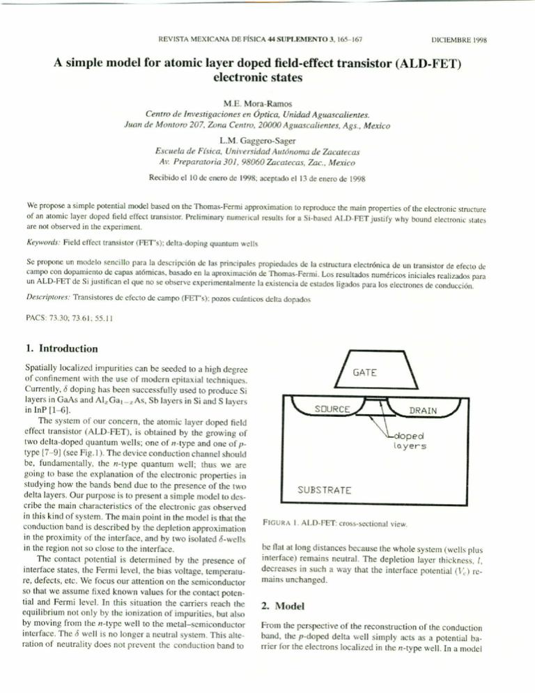
The syslem of our eoneem, lhe atomie layer doped field
effeel Iransislor (ALD-FET), is oblained by lhe growing of
two delta-doped quantum wells; one of Il.rypc and one of 1'_
lype [7-9] (see Hg.I). The device conduelion ehannel should
be, fundamenlaIly, lhe f1-1ype quanlum weIl; lhus we are
going to base the explanation of rhe elccrronic propertics in
sludying how the bands bend due lo Ihe presenee of lhe Iwo
delta layers. Qur purpose is lo presenl a simple model lo describe the main characteristics of rhe clectronic gas observcd
in lhis kind of syslem. The main point in Ihe model is Ihallhe
eonduelion band is deseribed by Ihe deplelion approximalion
in lhe proximily of the interface, and by two isolaled 6-weIls
in the region nOl so c10se lo the interfacc.
The eontael pOlenlial is delermined by lhe presenee of
inlerface states, the Fermi level, rhe bias volrage, tcmperalure, defecrs, etc. Wc focus our attention on rhe semiconductor
so thar wc assume fixed known values fOf rhe conlacr potcnti al and Fermi leve!. In this siruarion the carriers reach lhe
equilibrium nor only by the ionizarion 01"impuritics, but 3150
by moving from the Il-typc well lO the metal-semiconductor
interfacc. The 6 wcll is no longer a ncutral systcm. This alle.
ration of neutralily does not prevent the conduction band lo
/
GATE
\
SDURCE
DRAIN
doped
luyers
SUBSTRATE
FIGURA l. ALD-FET: cross-scctional
view.
be fla! at long disranccs becausc [he whole system (wclls plus
interface) rcmains neutral. The depletion layer lhickncss. t,
decreases in such a way lhar the interface potential (\'~) rcmains unchangcd.
2. Model
From the pcrspectivc of lhe reconstruclion of the condUClion
band, Ihe p-doped delta well simply aets as a potenlial barrier for thc electrons localizcd in the n-type well. In a model
166
ME MORA-RAMOS
previously proposed for 6-FET [10), lhe semiconduclor conduction band is descrihed lhrough a pOlenlial which has lhe
form al' a Schottky barrier plus a simple Thomas-Fcrmi cxpression for lhe ¡solaled n-Iype 6-well which was lirsl proposed in Ref 11. The question is lhal lhe p-Iype 6-well can also
he veey weH dcscrihcd within (he Thomas-Fermi approximalion as has becn shown in Ref. 12. Thcrcfore. wc propase
(he following cxprcssion as a pOlcntiai moJel lo dcscrihe the
semiconductor conduction band in the ALD-FET:
V(=)
=
+ [\~,(=) + I'p(Z)]8(/d - z).
I'sch(Z)
if=2:0,
if Z < 0,
fr\'c
lf bound-negativc
cnergy-states
occur in the systcm.
the quantity Id will represcnt the zera potcntial position, l.e..
we assumc that the well docs not contributc to the total potential in the region of the ionized impuritics. Thereforc, in
our mode11d is also thc depletion layer width because alzcro
tempcraturc only the impuritics helow the Fermi level (£1')
are ionized.
Thc proposed potential model satisfies the boundary conditions and describes in a simple way the esscntials of the
actual physical system. Il will be used to sludy the elcctranic
structure and can be the starting potential for a more exaet
selfconsistent calculation.
Since' the tcmperature to he considereJ is c10se 10 zera.
the cnergy levels ¡hat we take ¡nlo account are only those bclow lhe Fenni level which, following ¡oriaui [111 wc lake al
the conduction band edgc.
(4)
The pOlenlials 01'. lhe p- and n-lype delta-doped quanlum wclls in the Thomas-Fcrmi aproximation
are. rcspcctively [10-121:
(5)
(6)
\~.(z) - Ep =
3/2
mhh
e'
11
=--
r,.
2r,,,3 ) 1/5
( rre2]J2D
(7)
and
e2 (m,;)3/2
= -r,
=On
=
157fh
3
'
with
(8)
mili are the cffectivc masscs of the hcavy and
the Iight hales. rcspectivcly. m; is (he effcctivc mass 01'the
conduction electrons.
HeTe, m/¡f¡ and
\Ve have slUdied a Si-based ALD-FET syslem, ano lhe 1'0lIowing values for the inpul parametcrs have beco used:
IHh/¡ = 0.5211/0. mIh
0.161110; m;
(m;l,nd)I/3 with
J1Id
= O.91G3mo and l11el
O.1905mo
(mo bcing free
c1ectran l11ass). On the other hand, the valuc tr = 11.7 is
taken.
The ¡¡rst step in the nUl11crical calculation is to look
for the non-trivial solutions of the trascendental cquation
I'(ld)
O. They indicale lhe exislance 01' a negalive pOlenlial
region and, consequenlly, lhe presence 01' bound energy slates which will have an associated two-dirnensional electron
gas responsible for a much higher speed operalion.
For that search. we eonsidcred values 01'.vd ranging [rom
0.1 x 101M cm-3 to 1 x 10¹⁸ crn-3.the contaet potential Ve
took values fmm 0.4 cV to 1 cV and the two-dimensional im+
purity conccntrations n2J) and J12D varied both fmm 3 x 10¹²
crn-:.l 10 ..¡ X 10H cm-2. Thc conclusion of the nurncrical
calculation with this potcntial model is that within those inlervals a Si-hased ALD-FET syslem does nol exhibil lhe prescnec of elcctronic localized states; i.e., the minirnun value
01"\1(..:) always remains positivc and the system beeomes a
Schottky barricr with an inhomogeneous distrihution 01"impuritics.
=
wilh
on
3. Results and conclusions
=
the paramclcrs bcing
°
concentra-
(2)
(he well known cxprcssion
2rre.2 Sd .
impurity
tiaos (l>2LJ and H2D. respcctivcly) are also two important pararneters to be fixed. Both usually have values bctwcen 1OJ:l
and 9 x 10Bcm-2.
Nd is the background impurily conccntralion; 1 is (he distance helween lhe inlerface and Ihe poinl heyond which Ihe field
ceeated by the charge al the interface is zera, and is givcn by
=
=
p- ano ll-typc
(1)
and
1
=
Thc tWQ-dimensional
where
8(=)={~
Thc lirsl question lo clarify is welher bolh wells are in faet
too clase. In that case, the rccombination of donar ano acceptor impurilics might aCCUf, and (ha! is an undcsirablc cffect.
So, the scparation distance betwccn both wclls has to be-al
Icasl-grcater (han the sum of the cffeclivc Uohr radius corresponding la the f1-typc impurities plus the corresponding
la the p-lypc impurities. In the work. wc fix lhis scparation as
200 Á. in such a way Ihat the nUlllcrical cvaluation has beco
performed for 6"
300 A, and 6"
500 A.
Re •.. Mex.l-"ís. +lS3(1998)
165-167
=
=
A SIMPLE MODEL FOR ATOMIC LAYER DOPED FIELD-EFFECTTRANSISTOR
The existance of discrele energy levels for the conduction
clcctrons would Icad to an important qualitalive changc in the
physics of Ihis kind uf device. It is necessary lo explore olher
physically realistic (and experimenlally achievahle) intervals
(ALD-FET) ELECTRONIC
STATES
167
for the paramClcrs as well as for the separation bctwccn the
lO make a definitive conclusion. 01' coursc,
another possibilily is lhe use of a differenl malerial (GaAs.
for inslance) lo be lhe basis of Ihe ALD-FET syslelll.
Ó laycrs. in order
1. E.F. Schubert. A. Fischcr. and Klaus Ploog, IEEE Transaclioll.S
on Electron Del'ices ED-33 (1986) 625.
7. K. Yamaguchi, Y. Shiraki. y. Katayama. and Y. Murayamn.
J,m. J. AI'I". I'hys. 5uppl. 22.( (1983) 267.
2. S.L. Wu. T.K. Carns. S.1. Wang. and K.L. Wang. A[J[JI. Phys.
Lell. 63 (1993) 1363.
8. A.A. van Gorkum, K. Nakagawa. and Y. Shiraki.
I'hys. 26 (1987) L 1933.
3. t\1. Santos, T. Sajata. A.~1. LanziJloto. and "-1.Shayegan. Sur!
Sci. 228 (1990) 255.
4. E.E Shubert, J.B. Stark, T.H. Chiu. and 8. Tcil. App/. Phy.\'.
Lell. 53 (1988) 293.
J[JtI.
1. AI'I'I.
9. K. Nakagawa. A.A. van Gorkum. and Y. Shiraki. Al'pl. Phys.
Le//. 54 (1989) 1869 .
10. L.M. Gaggcro-Sagcr
(1995) 4566.
and R. Pércz-Alvarcz, 1. Appl. Phys.
78
5. K. Kohler. P. Ganser. and M. Maier. J. Crysl. Growlh 127
(1993) 720.
11. L. Ioriaui.l'hys.
6. E.H. Rhoderick alld R.H. Williams, Me/al SemK'oluluclor
taelS. Second Edilion, (Clarendon Press. Oxford. 1988).
12. L.M. Gaggcro-Sager. M.E. Mora-Ramos. and D.A. Contrcras5010rlo.l'h.l's. Rev. B 51 (1998) 6286.
Curl-
ReI'. Mex. Fú. 44 53 (1998) 165-167
Rev. 841
(1990) 8340.
